Choose PCB Components for a Prototype
Printed Circuit Boards (PCBs) serve as the backbone of electronic devices, connecting and powering various components to make them function seamlessly. Whether you are a hobbyist or an engineer developing a new product, effective selection and placement of PCB components is essential to the success of your prototype. In this article, we will discuss the key factors to consider when selecting PCB components for your project, along with guidelines to follow during manufacturing.
Selecting the correct components is the most important step in building a functional prototype. To begin, clearly define your project’s functional requirements, considering things like power consumption, speed, size constraints, and environmental conditions. You will also need to determine the physical layout of your PCB, including its layer structure, component placement, and any industry-specific standards or certifications that apply.
To ensure that your PCB is constructed properly, it is important to choose the right footprint and land pattern for each of its components. The footprint refers to the set of pads on a circuit board that are used to physically attach and electrically connect a component. The land pattern is the setup of these pads, and it is important that they match the configuration of leads on the component.
Once you’ve finalized your component selection and layout, you can move on to preparing the Gerber files for your PCB fabrication. This process includes ensuring that the file is properly formatted and containing all of the necessary information for its production. Once the files are ready, you can submit them to a PCB manufacturer for fabrication and prototyping.
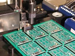
How to Choose PCB Components for a Prototype
When creating a PCB, it’s important to keep in mind that space is limited. This means that you will need to carefully plan out the layout of all of your components, leaving enough space for traces and additional layers as needed. Additionally, you’ll want to avoid placing too many components near each other, as this can lead to signal interference.
Another important factor to consider when choosing PCB components is the optimum thermal management of your circuit. As electricity flows through the circuit, it creates heat that can cause damage to the components if not properly managed. To avoid this, you should design your layout to include adequate heat venting techniques and use proper grounding methods.
As you work on your PCB assembly, it is important to carefully inspect the prototype printed circuit board assembly for visual defects and quality issues. You should also perform a series of tests using equipment like oscilloscopes, multimeters, and thermal cameras to ensure that the prototype is functioning as intended. Identify any issues or anomalies and make iterative adjustments to your schematic or layout until you are satisfied with its performance.
By following these simple tips, you can ensure that your PCB will function as expected and meet all of your design requirements. With careful planning, careful testing, and the help of a reliable PCB prototype manufacturer, you can be confident that your prototype will be ready for production.